HW-274 on the lower silkscreen). Other FX2LP clones share the same chip but may relabel or reorder header pins — always cross-check your own board's silkscreen against the photo and tables below.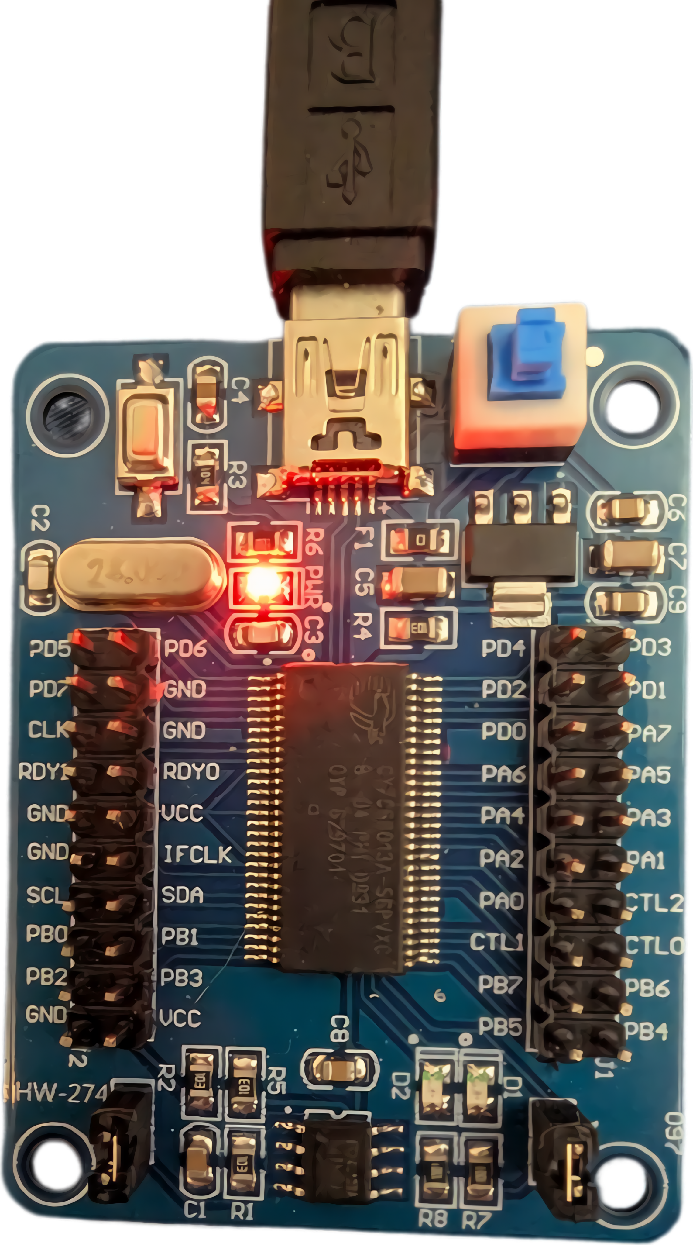
1. What this thing is
The CY7C68013A is a USB 2.0 High-Speed (480 Mbps) microcontroller built around an enhanced 8051 core with a fast parallel "GPIF/Slave-FIFO" interface. It is the heart of the inexpensive blue/black breakout boards sold as "24 MHz 8-channel USB logic analyzers" and as "EZ-USB FX2LP development boards."
Out of the box, with no EEPROM image programmed, it enumerates on a host PC as:
04b4:8613 Cypress Semiconductor Corp. CY7C68013 EZ-USB FX2 USB 2.0 Development Kit
That default identity is a blank slate. The board becomes whatever firmware is loaded into it — either permanently (written to the on-board I²C EEPROM) or temporarily (uploaded into RAM over USB at runtime):
| Firmware loaded | The board becomes… |
|---|---|
fx2lafw (sigrok) | A logic analyzer — 8 channels, up to 24 MS/s. The most common use. |
| Vendor / custom 8051 code | A USB-to-SPI / I²C / JTAG bridge, or a general 8051 dev board. |
| None | The raw 04b4:8613 device, awaiting an upload. |
fx2lafw into the chip's RAM on the fly every time you scan — you do not have to permanently flash anything to use it as a logic analyzer.2. The HW-274 board layout
The HW-274 routes the FX2's I/O ports to two pin headers — one on each side of the chip — rather than four separate port blocks. Below is the silkscreen as printed on the board (read directly from the photo above). Pins are listed top → bottom as the board sits with the USB connector at top.
(?). Confirm against your unit before wiring — and if yours differs, that's useful feedback for this repo.Left header (outer / inner columns)
outer   inner
PD5     PD6
PD7     GND
CLK     GND
RDY1    RDY0
GND     VCC
GND     IFCLK
SCL     SDA
PB0     PB1
PB2     PB3
GND     VCC
Right header (inner / outer columns)
inner   outer
PD3     PD2
PD1     PD0
PD0(?)  PA7
PA6     PA5
PA4     PA3
PA2     PA1
PA0     PB6
PB7     CTL1(?)
CTL0    PB5
PB5(?)  PB4
The HW-274 exposes Port A (PA0–PA7), Port B (PB0–PB7), Port D (PD0–PD7), the I²C bus (SCL/SDA, to the EEPROM), clock/ready lines (CLK, IFCLK, RDY0/RDY1), GPIF control (CTL0/CTL1), and power (VCC = 3.3 V, GND). Note Port C is not broken out on this board.
The generic FX2LP port model (for reference)
Underneath the HW-274's labels, the FX2's four 8-bit ports map to the standard roles below — useful for understanding what each pin does electrically.
Full header reference
| Header / Pin | Count | What it is | Logic-analyzer role |
|---|---|---|---|
| PB0–PB7 | 8 | Port B — FIFO data byte 0 | Capture channels CH0–CH7 (the 8 inputs you probe with) |
| PD0–PD7 | 8 | Port D — FIFO data byte 1 | Channels 8–15, only with 16-ch firmware. Default fx2lafw = 8 ch on PB. |
| PA0–PA7 | 8 | Port A — control / GPIO. Several pins double as FIFO control (FLAGA, SLOE, SLRD, SLWR, PKTEND). | General I/O; not used by basic capture. |
| PC0–PC7 | 8 | Port C — general-purpose I/O | Unused by basic logic analyzer. |
| GND | 2+ | Ground | Common ground to the target — mandatory. |
| 3V3 / VCC | 1+ | 3.3 V rail, regulated on-board from USB 5 V | Voltage reference only. Do not back-feed. |
| 5V / VBUS | 1 | USB bus 5 V in | Rarely needed externally. |
| CTL0–2, RDY0/1 | few | GPIF / Slave-FIFO handshake lines | Unused for capture. |
| SCL / SDA | 2 | I²C bus to the configuration EEPROM | Firmware / EEPROM programming only. |
| RESET / WAKEUP | 1–2 | 8051 reset / USB remote-wake | Leave alone. |
3. Electrical specs (the numbers that matter)
Logic levels
- I/O is 3.3 V CMOS.
- Inputs are NOT 5 V tolerant — do not feed 5 V signals in.
- VIH ≈ 2.0 V, VIL ≈ 0.8 V.
- Reads 1.8 V signals fine as a passive listener (1.8 V > VIH threshold for "high" is marginal — verify per target).
Capture limits (as fx2lafw LA)
- Channels: 8 (on PB), 16 with special firmware.
- Max sample rate: 24 MS/s (8-ch). Higher rates reduce channel count.
- No on-board sample memory — streams live over USB, so sustained rate is USB-bound.
- No analog, no protocol triggering in hardware (PulseView does software decode).
4. Using it as a logic analyzer
Software setup (Linux)
sudo apt install sigrok pulseview sigrok-firmware-fx2lafw

# Plug the board in, then confirm it is seen and fx2lafw uploads:
sigrok-cli --scan
#   expected:  fx2lafw - 8 channels: D0 D1 D2 D3 D4 D5 D6 D7
If --scan shows fx2lafw with 8 channels, you're ready. Open PulseView, select the device, set the sample rate and count, and hit Run. Add a protocol decoder (SPI, I²C, UART, etc.) from the toolbar to turn raw traces into decoded bytes.
Wiring example — sniffing an SPI bus
| FX2 pin | Connect to target signal |
|---|---|
| PB0 | SCLK (SPI clock) |
| PB1 | MOSI (controller → peripheral) |
| PB2 | MISO (peripheral → controller) |
| PB3 | CS / SS (chip select) |
| GND | Target ground — connect this first |
5. Safety & gotchas
fx2lafw keeps the pins as high-impedance inputs by default.6. Quick troubleshooting
| Symptom | Likely cause / fix |
|---|---|
Shows as 04b4:8613 but sigrok-cli --scan finds nothing | Missing sigrok-firmware-fx2lafw package — install it, replug. |
| Not detected at all | Bad/charge-only USB cable, or a permissions issue — try with sudo or add a udev rule. |
| Captured traces are all flat / all high | No common ground with target, or probing the wrong pins. |
| Decoder output is garbage | Sample rate too low (raise to ≥4× signal clock) or decoder channel mapping is wrong. |
| Want it permanent | Write fx2lafw to the I²C EEPROM with cycfx2prog / fxload (advanced; not required). |